Freescale 公司的MD7IC2050N是RF LDMOS寬帶功率放大器,工作頻率從1750到 2050 MHz,多級結構的工作電壓從26V到32V,平均輸出功率10W,功率增益高達30dB,片內50歐姆匹配輸入,集成了ESD保護, RoHS兼容,適用于所有蜂窩基站的調制格式.本文介紹了MD7IC2050N的主要特性,方框圖以及MD7IC2050NR1(GNR1)(NBR1)測試電路元件布局圖和元件數值, MD7IC2050NR1(GNR1)(NBR1) 1880MHz測試電路元件布局圖和元件數值表.
RF LDMOS Wideband Integrated Power Amplifiers
The MD7IC2050N wideband integrated circuit is designed with on- chip matching that makes it usable from 1750 - 2050 MHz. This multi – stage structure is rated for 26 to 32 Volt operation and covers all typical cellular base station modulation formats.
Typical Doherty Single- Carrier W-CDMA Performance: VDD = 28 Volts,
IDQ1A = IDQ1B = 30 mA, IDQ2A = 230 mA, VG2B = 1.4 Vdc, Pout = 10 Watts Avg., Channel Bandwidth = 3.84 MHz, Input Signal PAR = 9.9 dB @ 0.01% Probability on CCDF.

Capable of Handling 5:1 VSWR, @ 32 Vdc, 2017.5 MHz, 79 Watts CW Output Power (3 dB Input Overdrive from Rated Pout)
Stable into a 5:1 VSWR. All Spurs Below -60 dBc @ 20 Watts to 80 Watts CW Pout
Typical Pout @ 3 dB Compression Point _ 74 Watts CW 1880 MHz
Typical Doherty Single- Carrier W-CDMA Performance: VDD = 28 Volts,IDQ1A = IDQ1B = 30 mA, IDQ2A = 230 mA, VG2B = 1.4 Vdc, Pout = 10 Watts Avg., Channel Bandwidth = 3.84 MHz, Input Signal PAR = 9.9 dB @ 0.01% Probability on CCDF.

MD7IC2050N 主要特性:
100% PAR Tested for Guaranteed Output Power Capability
Production Tested in a Symmetrical Doherty Configuration
Characterized with Series Equivalent Large-Signal Impedance Parameters and Common Source S-Parameters
On-Chip Matching (50 Ohm Input, DC Blocked)
Integrated Quiescent Current Temperature Compensation with Enable/Disable Function
Integrated ESD Protection
225C Capable Plastic Package
RoHS Compliant
In Tape and Reel. R1 Suffix = 500 Units per 44 mm, 13 inch Reel
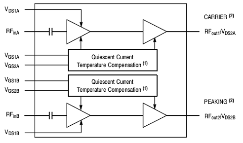
圖1.MD7IC2050N功能方框圖
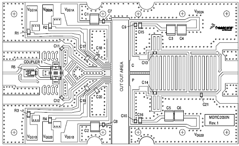
圖2.MD7IC2050NR1(GNR1)(NBR1)測試電路元件布局圖
MD7IC2050NR1 (GNR1)(NBR1) 測試電路元件數值表:
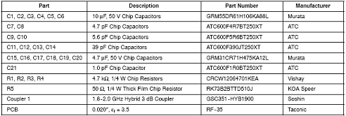
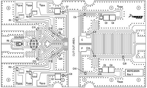
圖3.MD7IC2050NR1(GNR1)(NBR1) 1880MHz測試電路元件布局圖
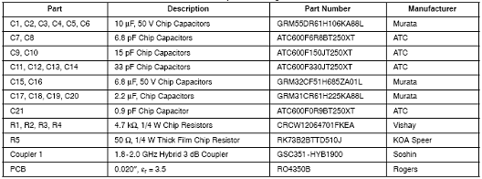
MD7IC2050NR1(GNR1)(NBR1) 1880MHz測試電路元件數值表:
詳情請見:
http://www.freescale.com/files/rf_if/doc/data_sheet/MD7IC2050N.pdf
RF LDMOS Wideband Integrated Power Amplifiers
The MD7IC2050N wideband integrated circuit is designed with on- chip matching that makes it usable from 1750 - 2050 MHz. This multi – stage structure is rated for 26 to 32 Volt operation and covers all typical cellular base station modulation formats.
Typical Doherty Single- Carrier W-CDMA Performance: VDD = 28 Volts,
IDQ1A = IDQ1B = 30 mA, IDQ2A = 230 mA, VG2B = 1.4 Vdc, Pout = 10 Watts Avg., Channel Bandwidth = 3.84 MHz, Input Signal PAR = 9.9 dB @ 0.01% Probability on CCDF.

Capable of Handling 5:1 VSWR, @ 32 Vdc, 2017.5 MHz, 79 Watts CW Output Power (3 dB Input Overdrive from Rated Pout)
Stable into a 5:1 VSWR. All Spurs Below -60 dBc @ 20 Watts to 80 Watts CW Pout
Typical Pout @ 3 dB Compression Point _ 74 Watts CW 1880 MHz
Typical Doherty Single- Carrier W-CDMA Performance: VDD = 28 Volts,IDQ1A = IDQ1B = 30 mA, IDQ2A = 230 mA, VG2B = 1.4 Vdc, Pout = 10 Watts Avg., Channel Bandwidth = 3.84 MHz, Input Signal PAR = 9.9 dB @ 0.01% Probability on CCDF.

MD7IC2050N 主要特性:
100% PAR Tested for Guaranteed Output Power Capability
Production Tested in a Symmetrical Doherty Configuration
Characterized with Series Equivalent Large-Signal Impedance Parameters and Common Source S-Parameters
On-Chip Matching (50 Ohm Input, DC Blocked)
Integrated Quiescent Current Temperature Compensation with Enable/Disable Function
Integrated ESD Protection
225C Capable Plastic Package
RoHS Compliant
In Tape and Reel. R1 Suffix = 500 Units per 44 mm, 13 inch Reel

圖1.MD7IC2050N功能方框圖

圖2.MD7IC2050NR1(GNR1)(NBR1)測試電路元件布局圖
MD7IC2050NR1 (GNR1)(NBR1) 測試電路元件數值表:


圖3.MD7IC2050NR1(GNR1)(NBR1) 1880MHz測試電路元件布局圖
MD7IC2050NR1(GNR1)(NBR1) 1880MHz測試電路元件數值表:

詳情請見:
http://www.freescale.com/files/rf_if/doc/data_sheet/MD7IC2050N.pdf

 粵公網安備 44030902003195號